We are specialists in quality batteries. We have batteries, chargers and accessories for everything you can think of. Low prices, big inventory, expert advice. Find your battery here!
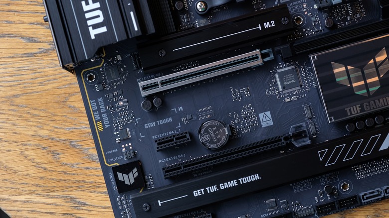
PC components have a finite number of channels that connect with the CPU. These channels are physically built into the CPU, the motherboard, and the components themselves — and they’re called PCIe lanes. Every GPU, SSD, or creator card you plug into your motherboard needs to send data to the CPU to function, and it does that through these PCIe lanes.
Every CPU has a fixed number of PCIe lanes, which dictate the bandwidth and are listed as x4, x8, x16, or x20 in spec sheets and user manuals. Plugging components into the PCIe slots uses up those lanes. The GPU, for instance, is usually installed into the primary x16 slot for the most bandwidth. If you have an M.2 SSD, that will use up four additional lanes, taking up a total of 20.
If your CPU only offers 20 lanes, any additional GPUs or SSDs will be routed through the motherboard’s PCIe lanes, which are still connected to the CPU, but indirectly. This is lane sharing in action, and it can slow things down without most users being aware. If you have PCIe 5.0 hardware and want to get full Gen 5 speeds, you’ll need full support across the board — that means a CPU, motherboard, and device with native Gen 5 support. But even then, your setup might not run at full speed if PCIe lanes become the bottleneck.
AMD Ryzen CPUs offer more Gen 5 lanes than recent Intel CPUs
As of this publication, only AMD’s Ryzen 7000 and 9000-series chips offer full PCIe Gen 5 bandwidth without lane sharing. These CPUs offer 28 Gen 5 PCIe lanes total — enough for a GPU in an x16 slot and at least one PCI 5.0 5 NVMe SSD to run at max speeds. Intel’s 12 trough 14th-gen CPUs only offer 16 Gen 5 lanes for graphics and an NVMe to split. That means Intel’s Alder and Raptor Lake CPUs can’t run a Gen 5 GPU with a Gen 5 SSD at full speeds without lane sharing at the same time.
If you do install both a Gen 5 SSD and a GPU on Intel, something has to give — the SSD gets its full four lane bandwidth, but the GPU starts running at x8 instead of x16. With no SSD in the first M.2 slot, the GPU will use all 16 lanes. But if you drop even a Gen 4 SSD in the top PCIe x4 NVMe slot – that shares lanes with the GPU — on an Intel system, the GPU will still drop to x8. This is especially relevant for cards like the Radeon RX 9000 series and the RTX 50 series, which are designed to take full advantage of Gen 5 natively.
How to check if your SSDs are hurting your GPU performance
AMD gives you the most Gen 5 lanes upfront, but you’ll still need at least a B650e motherboard to actually make use of them. Entry-level B650 boards don’t offer Gen 5 M.2 slots at all, and even on high-end X870E motherboards — which come with up to three Gen 5 NVMe slots — the lane layout matters. Board documentation from Asus shows how lane sharing works on the X870E with different PCIe slots occupied: if you use the third M.2 slot, the first PCIe x16 Gen 5 slot drops to x8, and the second starts running at x4.
At eight lanes, that is still equal to x16 bandwidth of a PCIe 4.0 slot, and x8 for the second slot. If both the second and third M.2 slots have SSDs in them, that second PCIe x16 slot gets disabled entirely. Thankfully, the real-world impact is smaller than it seems — for gamers, at least. Gamers Nexus tested this with an RTX 5090 and found that dropping from Gen 5 x16 to Gen 3 x16 only resulted in a 1-4% performance loss in modern games.
However, if you still want to check your GPU’s PCIe lane configuration, use a software like CPU-Z — it’s easier than going through your motherboard manual. Just go to the “Mainboard” tab and look for the “Graphic Interface” section. Under the “Bus” block, check if the “current link width” link width matches the “max supported.” If they don’t match, your GPU is running at the lower of the two.
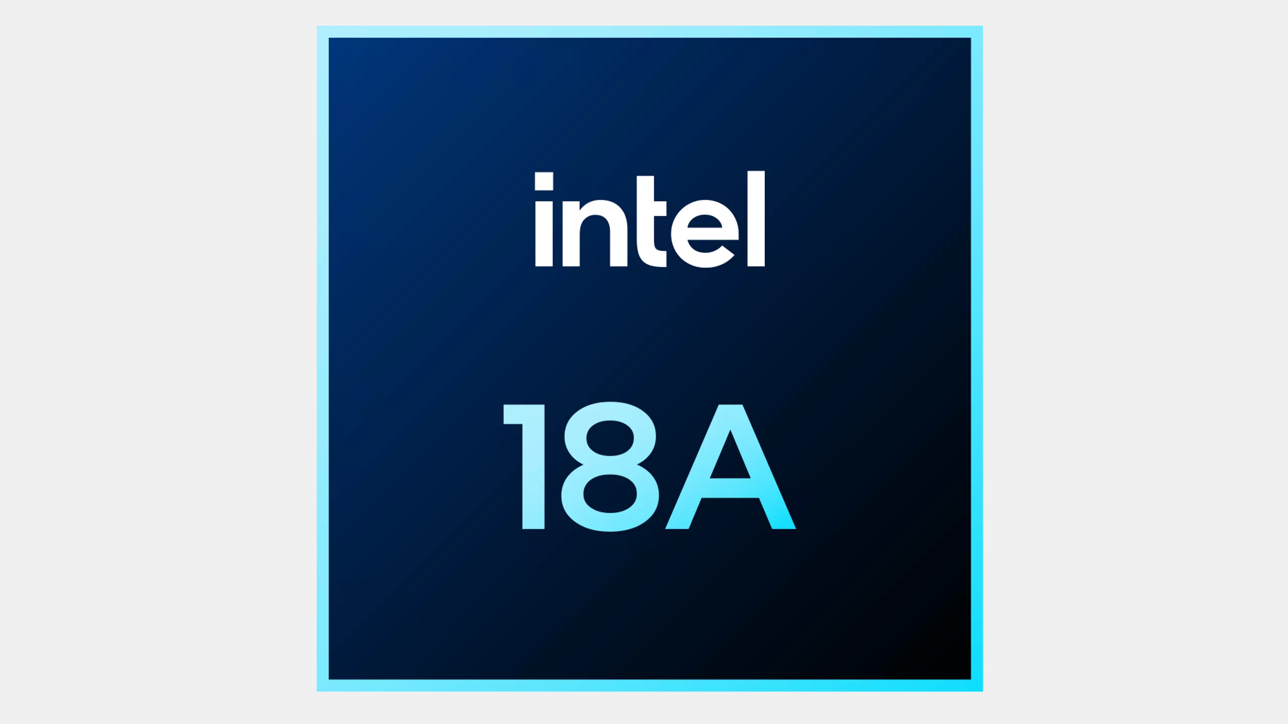
Intel has published a paper about its 18A (1.8nm-class) fabrication process at the VLSI 2025 symposium, consolidating all its information about the manufacturing technology into a single document. The new 18A production node is expected to deliver significant improvements in power, performance, and area over its predecessor, increasing density by 30% while enhancing performance by 25% or reducing power consumption by 36%.
But, perhaps more importantly, 18A will be Intel’s first process technology in years that will compete head-to-head with TSMC’s leading-edge technology when both enter mass production in the second half of this year.
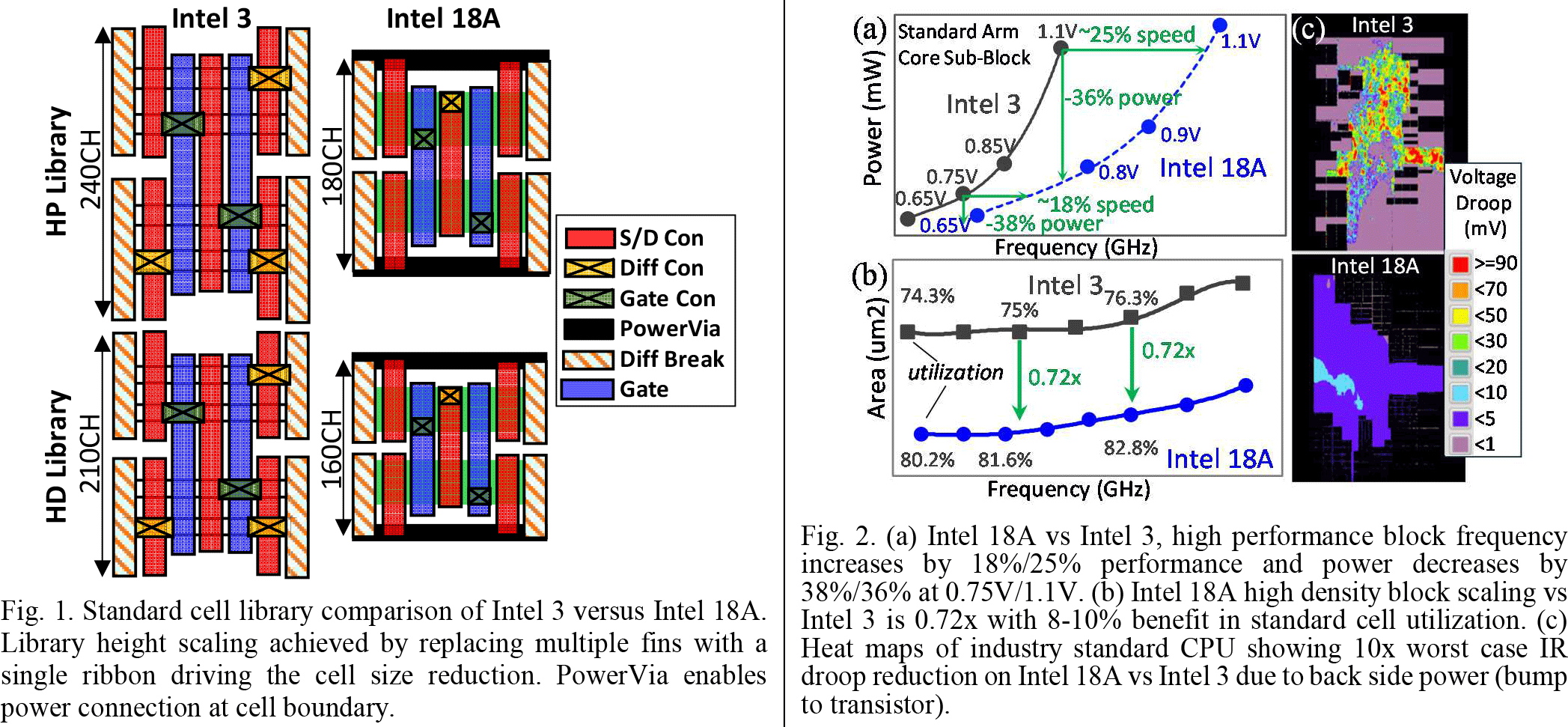
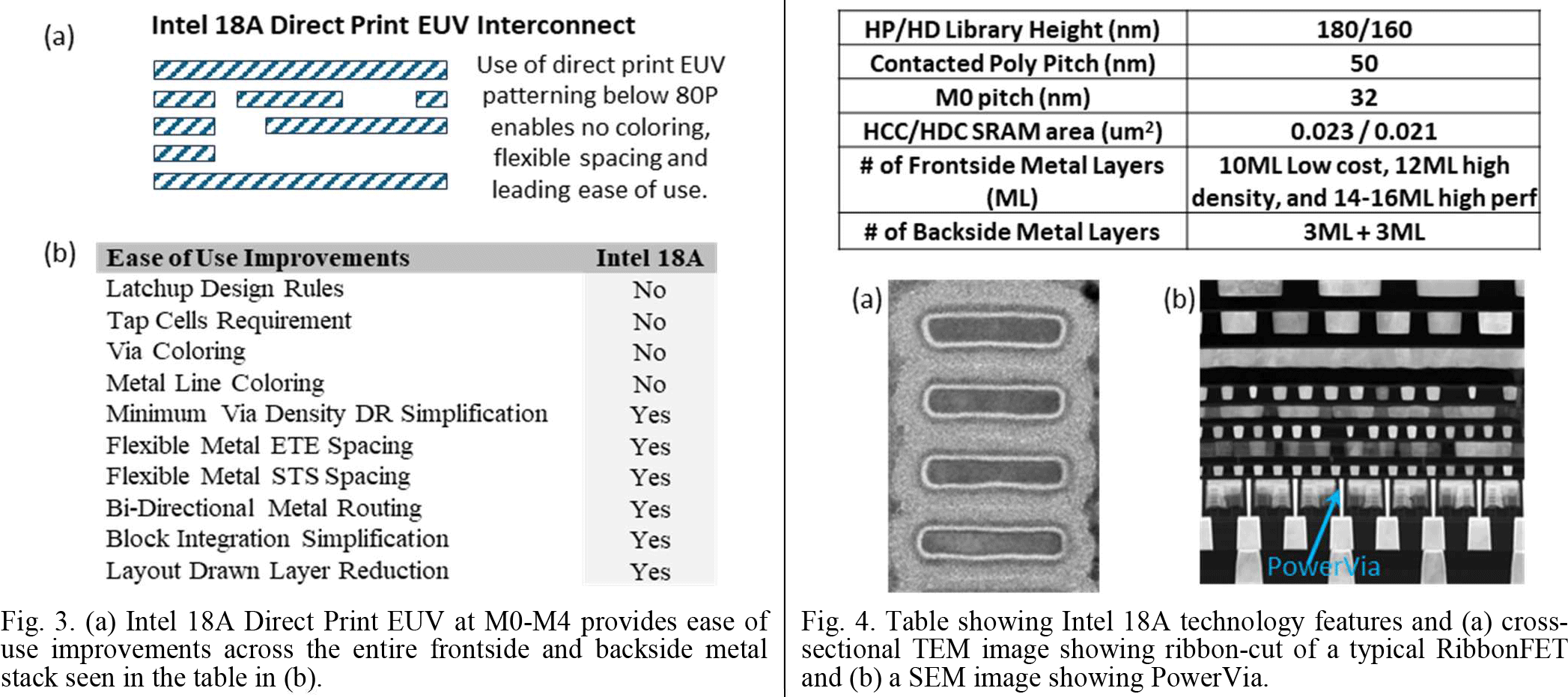
Intel’s 18A process node is designed for a wide range of range of products across both client and datacenter applications, and the first Intel’s product to use it will be the Panther Lake CPU, which is due to be formally announced later this year. To address different applications, Intel 18A has two libraries: high-performance (HP) with 180nm cell height (180CH) and high-density (HD) with 160nm cell height (160CH) for lower-power applications.
How 18A stacks up against previous nodes
Intel 3 vs Intel 4
18A vs Intel 3
Power
?
36% (at 1.1V) – 38% (at 0.75V)
Performance
18% (?)
18% (at 0.75V) – 25% (1.1V)
Density
–
1.3X
SRAM Cell Size
0.024 µm²
0.021 µm²
Transistor
FinFET
RibbonFET GAA
Power Delivery
Front-side
PowerVia BSPDN
HVM
mid-2024
H2 2025
Intel says that compared to Intel 3, its 18A fabrication technology boosts performance by 25%. It manages to achieve this without increasing voltage or circuit complexity when running a typical Arm core sub-block, implemented using a 180CH HD library at 1.1. When operating at the same clocks and 1.1V voltage, it also cuts power usage by 36% compared to the same design on Intel 3. At a reduced voltage of 0.75V, 18A offers an 18% speed increase and uses 38% less energy. Furthermore, designs fabricated on 18A occupy roughly 28% less area than those built with Intel 3.
(Image credit: Intel)
There is a major catch about comparison of voltages between Intel 3 and 18A. The former supports <0.6V, 0.75V, 1.1V, and 1.3V, which makes it particularly suitable for data center devices. This type of workload needs to burst to high clocks, across dozens of cores when demanding peak performance. Then, it’ll need to throttle down to a low-power state to save power. To contrast, 18A seems to support 0.4V, 0.75V, and 1.1V, which very good for client PCs and data center CPUs, but may not be ideal for processors that need maximum clock speeds. However, other advantages of Intel’s 18A will likely offset the lack of 1.3V support for the vast majority of applications (more on this later).
As for SRAM, Intel’s 18A process includes a high-density SRAM bit cell measuring 0.021 µm², translating to an SRAM density of roughly 31.8 Mb/mm². This is a major improvement over the 0.024 µm² bit cell used in Intel 4. This puts Intel 18A on par with TSMC’s N5 and N3E nodes in terms of SRAM density. However, TSMC’s upcoming N2 process goes further, reducing the bit cell to approximately 0.0175 µm² and achieving a higher density of around 38 Mb/mm².
Intel 7
Intel 4
Intel 3
Intel 18A
Contacted Poly Pitch
54nm/60nm
50 nm
50 nm
50 nm
Fin Pitch
34 nm
30 nm
30 nm
?
M0 Pitch
40 nm
30 nm
30 nm
32 nm
High Performance Library Height
408 nm
240 nm
240 nm
180 nm
High Density Library Height
–
–
210 nm
160 nm
HP Library Height x CPP
24.4K nm²
12K nm²
12K nm²
9K nm²
HD Library Height x CPP
–
–
10.5K nm²
8K nm²
Intel’s 18A relies on the company’s 2nd generation RibbonFETgate-all-around (GAA) transistors, and aPowerVia backside power delivery network (BSPDN). We investigate exactly how Intel managed to implement GAA transistors and BSPSN below.
In GAA transistors, the gate completely wraps around the channel, offering superior electrostatic control compared to FinFETs, which only wrap around on three sides. Such an architecture enables engineers to finely tune device characteristics for either high performance or low power consumption by adjusting the total effective channel width (Weff). This is typically achieved by varying the width and number of stacked nanosheets. More sheets, alongside wider sheets, can increase drive current and performance at the cost of power, while fewer or narrower sheets reduce both performance and power consumption.
(Image credit: Intel)
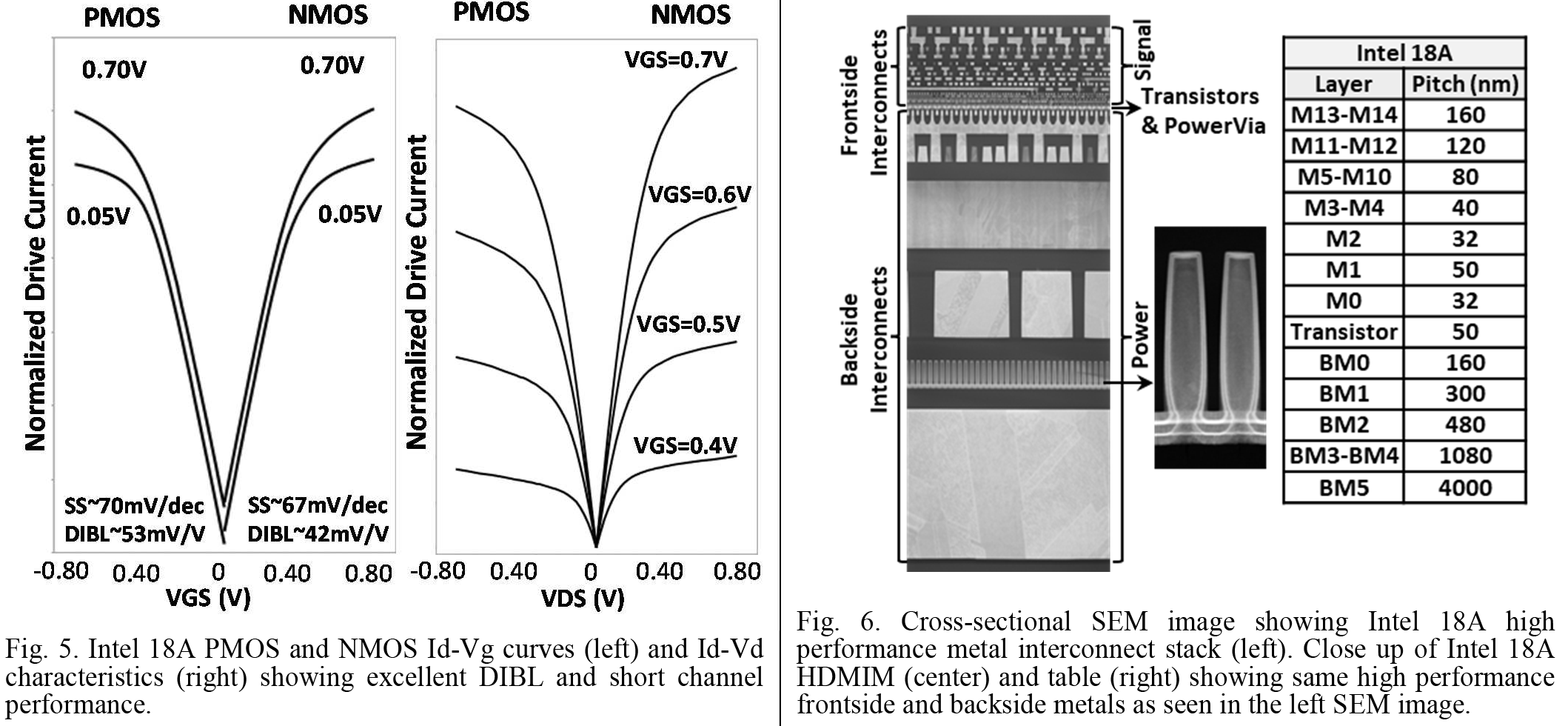
Intel’s 18A RibbonFET transistors feature four nanoribbons and support eight distinct logic threshold voltages (VTs) — four for NMOS, and four for PMOS — spanning a 180mV range. This level of VT granularity is achieved through dipole-based work-function tuning, a method that allows precise control of transistor behavior without altering its physical dimensions. This approach is especially important, given the tight spatial constraints in GAA transistor structures, such as RibbonFETs, where traditional methods, like doping adjustments, are limited.
An Intel graph from the paper shows that despite this wide VT range, the transistors exhibit strong electrical characteristics, including steep subthreshold slopes and well-behaved drive currents across both Id–Vg and Id–Vd curves. These results confirm that Intel has successfully maintained device performance and control across the entire VT spectrum, which enables flexible circuit design choices that balance frequency, power, and leakage within the same process.
Intel’s PowerVia backside power delivery network (BSPDN) relocates power delivery from the top metal layers to the rear side of the chip, creating a physical separation between power and signal wiring. This technique addresses issues like rising resistance in the vertical connections of in the back-end-of-line (BEOL) layers, which in turn enhances transistor efficiency and reduces power usage. Additionally, it prevents signal degradation caused by power interference and allows for tighter packing of logic elements, increasing overall circuit density.
(Image credit: Intel)
Intel’s PowerVia delivers power to transistor contacts, which is a slightly less sophisticated approach compared to TSMC’s Super Power Rail (coming in 2H 2026 along with A16), which connects directly to each transistor’s source and drain. In addition to BSPDN, Intel also implemented its new high-density metal-insulator-metal (MIM) capacitor to enhance power supply stability.
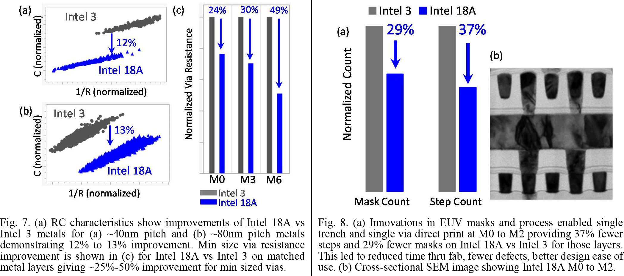
Intel has now disclosed the key benefits of its backside power routing. First up, PowerVia increases transistor density by 8% to 10%, which is quite a sizeable part of 18A’s overall 1.3X transistor density increase over Intel 3. Secondly, the front-side metal layers in its 18A process achieve approximately 12% better resistance-capacitance (RC) performance and show a 24% to 49% decrease in via resistance compared to Intel 3, thanks to improved metallization techniques and the use of ultra-low-k dielectrics. Thirdly, 18A’s PowerVia reduces voltage droop compared to Intel 3 (the worst-case scenario for Intel 3) by up to 10 times. Lastly, BSPDN simplifies chip design as it simplifies the routing of signal and power wires.
PowerVia’s reliability
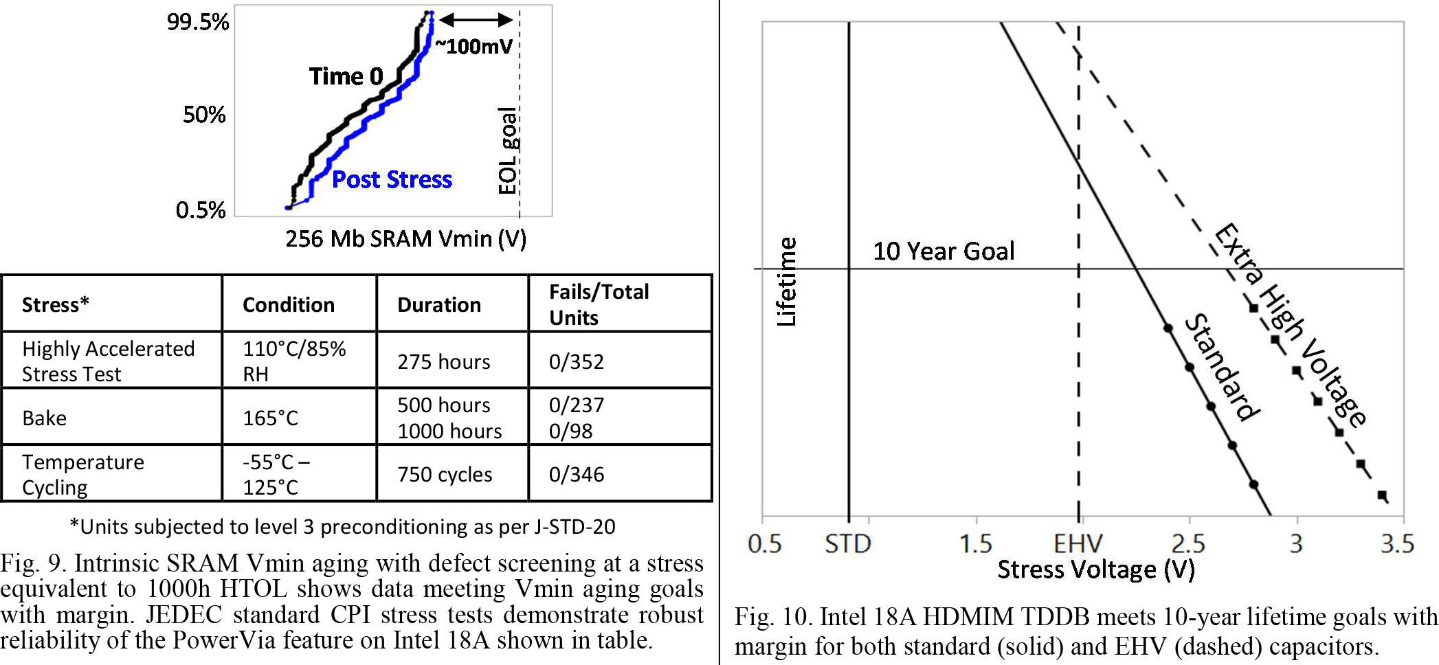
Since PowerVia is the industry’s first backside power delivery network (BSPDN) used in mass production, Intel also presented reliability test results. These demonstrate its long-term durability and chip-package interaction (CPI) performance.
(Image credit: Intel)
According to JEDEC-standard TQV tests, PowerVia passed multiple stress conditions with zero failures, including highly accelerated stress testing at 110°C and 85% humidity for 275 hours, extended high-temperature bake tests up to 1000 hours at 165°C, and 750 cycles of temperature swings from –55°C to 125°C. These results confirm that PowerVia can withstand harsh operating environments, without compromising structural or electrical integrity.
In addition to CPI reliability, Intel evaluated the impact of PowerVia on SRAM aging and performance stability. Under conditions equivalent to 1000 hours of high-temperature operation, SRAM arrays maintained stable minimum operating voltage (Vmin) with margin, showing no signs of degradation. This suggests that PowerVia does not negatively affect sensitive on-chip memory and is robust enough to support both digital logic and embedded SRAM under extended stress. Together, these findings are meant to affirm PowerVia’s readiness for deployment in high-performance, long-lifecycle computing platforms.
Manufacturability
In addition to improving performance, reducing power consumption, and enabling higher transistor density, Intel’s 18A simplifies production flows and simplifies chip design.(Image credit: Intel)
By moving power delivery to the backside, Intel eliminates the need for a front-side power grid, which, combined with direct EUV patterning, lowers the total number of masks and simplifies the front-end metal process. By using low-n absorber reticles with tailored dimensional adjustments, Intel also enabled single-pass EUV patterning for the M0–M2 metal layers. This simplification of the lower metal layers reduces process complexity and helps offset the cost of adding extra backside metal layers, which are based on mature, low-cost fabrication techniques. As a result, the overall design process becomes easier and cheaper.
In addition, the backside metal layers of 18A’s PowerVia are designed for low resistance and high thermal conductivity, which helps manage the increased power density from the GAA transistors. Also, carrier wafer bonding is optimized for heat removal through the backside, addressing the thermal challenges introduced by high-performance transistors. Finally, PowerVia is compatible with advanced packaging methods like Foveros and EMIB, though we already know this from the fact that Panther Lake uses 18A tiles as well as Foveros 3D.
Summary
Intel’s comprehensive technical overview of its 18A process node has highlighted the architecture, performance, and manufacturability improvements that position it as a competitor to TSMC’s upcoming N2. The 18A process introduces Intel’s second-generation RibbonFET (GAA) transistors and the industry’s first mass-production-ready backside power delivery network, PowerVia.
Together, these innovations enable up to 25% higher performance or 36% lower power consumption compared to Intel 3, while also increasing transistor density by about 30%.
Intel’s PowerVia contributes an 8–10% density gain, 12% RC improvement in metal layers, and up to 10 times lower voltage droop.
The new node has also passed stringent JEDEC reliability tests, including 1000-hour high-temperature aging and extensive thermal cycling to verify that it can be used for designs meant to work for a long time. Additionally, Intel further streamlined front-end patterning using single-pass EUV at M0–M2, thereby reducing mask counts and simplifying the design.
However, whether or not 18A can help Intel restore some of the lustre to its brand remains to be seen, as the company continues to wade its way through rocky waters.
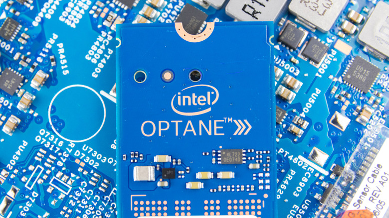
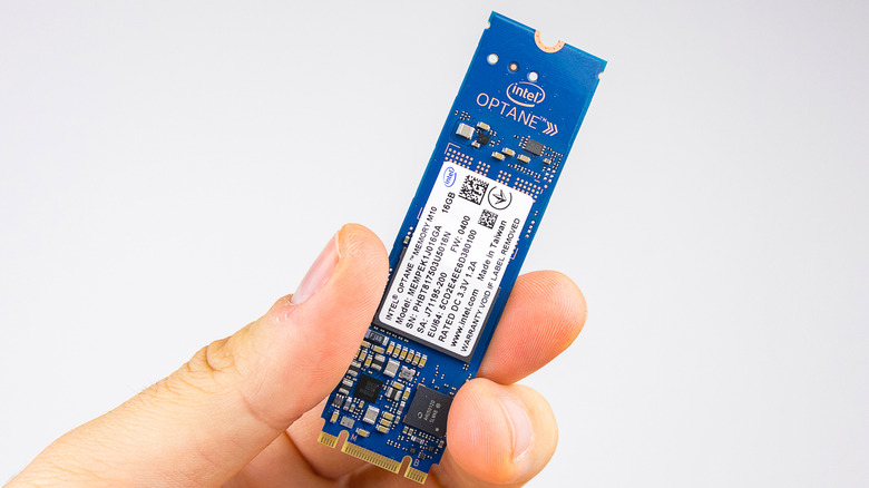
When Intel introduced its Optane memory solution, it was deemed the future of computing. “For the first time ever, we’ll be able to equip computers with memory that’s faster than NAND and more dense than DRAM, and nonvolatile,” the company said. Unfortunately, the product’s consumer market innings lasted merely half a decade before Intel pulled the plug on the whole endeavor. But, Intel is no stranger to killing products, both symbolic and strategic.
The cancellation of its highly ambitious AI chip project was also accompanied by the exit of company veteran and CEO, Pat Gelsinger, earlier this year. The same year, Intel put the NUC mini PC platform on cold ice. Intel even put an Atom chip inside an Android Wear smartwatch made by TAG Heuer, and then quietly abandoned those wearable ambitions. The list of dead and discontinued products at Intel is quite long, and nearly in the same league as the famed Google Graveyard.
With the Optane memory solution, the writing had been on the wall, at least from the market analysts’ perspective. To the last day, Intel was adamant that Optane was a tech stack ahead of its time, but it couldn’t evolve into a profitable business for the company. How much was the hit? Intel lost billions each year on the Optane business, and eventually had to write off assets worth over half a billion dollars when it announced its death.
Intel Optane was somewhat of a bridge between traditional RAM and storage modules, with the sole objective of speeding things up inside your computer. Intel officially referred to it as a system acceleration solution that would spped up data transfer between SSDs and the processing unit. The net result of those memory and storage innovations was faster boot time, quicker search and discovery of assets, quicker app launch, and overall enhanced responsiveness on Optane-powered machines.
At the heart of it was the non-volatile, dense 3D XPoint memory, which was achieved using sliced submicroscopic layers connected by perpendicular wires and stacked to enhance the memory density into a single, small package. Now, this tech was jointly developed by Intel and memory giant Micron. In 2021, Macron announced that it was shutting down development of 3D XPoint memory. The same year, Intel revealed that it was killing the Optane SSD platform built atop the PCIe 4.0 bus standard. By the end of 2021, Intel had sold its SSD and NND memory business to Korean memory chip giant, SK Hynix.
A few weeks later, Intel chief Gelsinger explained in an interview why he wanted the company to dump its memory business. “I never want to be in memory,” he told Stratechery. Months later, Intel announced in its Q2 2022 earnings that it was winding down its Optane business, which resulted in an inventory write-off worth $559 million. Intel didn’t outright reveal why, but in a statement shared with the press, the company hinted that it was not a “sufficiently profitable” venture.
If you are still rocking a computing machine, such as a laptop powered by 11th Gen Intel processors and the Intel Optane SSD solution, you are “temporarily” fine. On the operating system side of things, Intel says the Optane memory is compatible with the 64-bit version of Windows 11 and 10. However, if you haven’t made the jump to Windows 11 yet, prepare for the shift. On October 14, 2025, Microsoft will end official support for Windows 10.
If you invested in an Intel Optane-powered computing machine, the company will honor the standard 5-year warranty, calculated from the date of purchase. But do keep in mind that Intel is no longer offering services related to Optane products. For example, if you purchased a product with one of Intel’s Optane 8 and 9 series SSDs, they have already reached the End of Servicing (ESU), End of Life (EOL), and End of Interactive Support (EOIS) deadlines, as of 2024.
Similar is the status of Intel Optane H and M-series memory solutions. The sole exception is the Intel Optane Persistent Memory 100 Series, which is going to reach the EOIS status on June 30, 2025. Notably, Intel had already ceased to provide firmware updates and the necessary software tools for storage and memory tools in March this year. In a nutshell, your Optane machine will continue to work, but don’t expect a fix if something is broken, and of course, don’t buy any fresh Optane hardware.
 (Image credit: Intel)